Abstract
Over the course of a long time, all are searching for a good candidate to bridge the performance gap between high-speed but volatile DRAM and long latency yet non-volatile block storage devices, e.g., solid state drives and hard disks. Storage Class Memory, so called SCM, is deemed as a disruptive technology that embraces both good properties of byte-addressability, low-latency, and non-volatility. However, SCM till has the endurance problem, i.e., number of writes to the same location is limited. Even though a lot of innovative and successful controller designs can be seen in NVM-based, e.g., NAND flash, storage products, those design experience cannot be directly applied to the controller for SCM. One of major challenges is that traditional address-translation approaches will take a significant cost on table maintenance when SCM is served as a memory product and the access unit is 64 bytes (typical cache line size). In this paper, a table-less design for SCM controller is proposed to tackle the endurance problem and deliver superior performance in terms of access speed.
I. Introduction
NAND flash and DRAM have seen tremendous growth in volume and revenue recently, thanks to their wide applications in consumer devices as well as enterprise data centers. SSDs, built by NAND flash, have reduced the storage response time to micro-seconds from mille-seconds using HDD. However, there is still a three order of magnitude gap in performance between DRAM and NAND flash.
It is widely sought as an ideal device that has the response time and byte-addressable property of the memory, and the capacity and non-volatile property of the storage This kind of memory is generally referred to as the Storage Class Memory (SCM) [1]. In the past many years, there were numerous attempts by different companies and research groups to develop SCMs using different materials, processes, and circuit technologies. Some of the most prominent examples of SCMs to date include Phase Change Random Access Memory (PCRAM), Resistive Random Access Memory (RRAM), and Spin-transfer torque Magnetic Random Access Memory (STT-MRAM). In 2015, Intel and Micron announced 3D XpointTM, that is claimed to be “1000 faster than NAND flash and 10 times denser than DRAM [2]. In 2017 and 2018, Intel further made product announcements based on 3D Xpoint technology, OptaneTM SSD which is a block storage device, and Optane DC Persistent Memory™ which has a memory device [3].
In this paper, we are concerned with the design of an SCM controller. Based on our studies and results, we came to believe that a new type of controller is needed for SCM and that is different from an NAND flash controller. In Section II, we highlight the two main reasons why SCM controller should be different: 1) hardware architecture for performance, and 2) different needs for address mapping and wear leveling. In Section III, we describe the controller prototype that we built and the results we obtained. In Section IV, we conclude the paper.
II. Architecture reasons for a new SCM controller
Traditionally, a NAND flash controller is firmware-based in the sense that data movement is handled by hardware engines, but the “policy” of such data movement is implemented in firmware. For flash translation layer (FTL) [4], certain statistics such as cold/hot data take a long time scale to collect and process, and only firmware is suitable to do the task. Some background tasks such as garbage collection may also need flexibility to adapt its algorithms to the current state of the SSD. For the NAND channel controller, a firmware implementation can also allow the controller ASIC to support multiple NAND flash vendors or different generations of the NAND flash by firmware modification.
A firmware based architecture has an inherent disadvantage in performance, but for NAND flash, the advantage of flexibility outweighs the performance disadvantage. The reason is that the NAND flash device is relatively slow. For NAND channel controller, the firmware dispatches tasks to the hardware engines in the range of once every several micro-seconds. For FTL, the throughput rate depends on the I/O oprations per second (IOPs) requirement. For 100K IOPs, which is typical for SSD, the FTL firmware needs to handle one host request every 10 micro-seconds (in addition to the background tasks it needs to do as well). But overall such performance level is achievable by embedded controllers such as ARM etc. For high-performance, all-flash-array controllers, often times the high-performance server CPUs are used as controllers.
One of the key attributes of SCM is that its media latency is much smaller than that of NAND flash, roughly in the order of 100-300 nano-seconds, depending on read or write operation. For SCM channel controller, a firmware-based implementation cannot keep up with the media speed. For FTL (or more correctly SCM translation layer), the IOPs target can easily be in the order of 1M or higher. Such a performance level is also very challenging for a firmware-based architecture to achieve. Hence, though flexibility is still highly desirable, the performance requirement of a SCM controller simply renders a firmware-based architecture infeasible.
SCM controller needs a new architecture also because the requirement for address mapping and wear leveling is different for SCM. As the NAND flash, SCM also has finite (though better) write endurance and therefore requires address mapping and wear leveling.
NAND flash uses a table to map the logical address (which the application program wants to write to) to the physical address (which the NAND flash actually writes to). The same logical address could be mapped to different physical address at different time, and hence the wear is leveled. SSD is a block storage device with an addressing unit of 4K-byte, and the mapping table can be constructed at about a size that is 0.1% of the storage size. (e.g., for 1 Terabyte SSD, the table is about 1 Gigabyte.) Since this table search is on the critical path of NAND flash memory access, the table is usually implemented by faster technology such as DRAM. During power outage, the table content needs to be saved in NAND flash, commonly using an energy cap to hold the power temporarily in the process.
Unfortunately, this table-mapping wear-leveling technique cannot be used for SCMs, which can be applied to not only the block storage device, but also a memory device such as NVDIMM. For the memory application, a much smaller addressing unit (often 64-byte) is used. If we attempt to adopt the table mapping wear leveling technique, the table size will become 6.4% (i.e. 64x larger than 4K-byte access) of the storage size and the associated energy cap will also be too large to be feasible.
In the next Section, we will describe some experimental results of a new SCM controller architecture that is hardware-based, and performs address mapping and wear leveling without using a table. Please note that our architecture is different from the Start-Gap wear leveling technique proposed by IBM in 2009 [5].
III. Experimental Results of A New SCM Controller
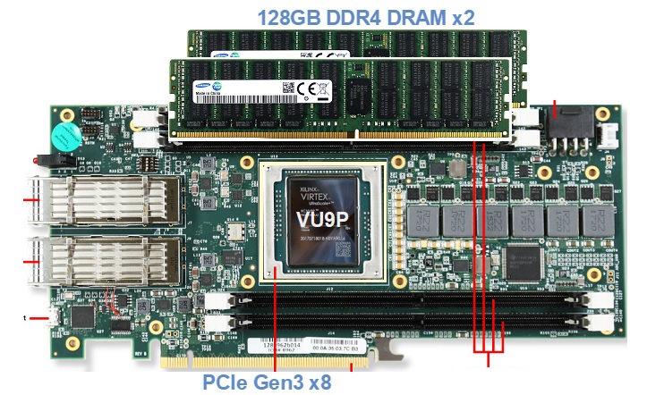
Fig. 1. VCU1525 platform
The experimental platform is built on Xilinx VCU1525 development kit, shown in Fig. \ref{fig/vcu1525}. The platform is composed of a Virtex UltraScale+ FPGA (VU9P) and two 128GB DDR4 DRAM’s, where DRAM is used to emulate 256GB SCM. The DRAM speed is limited to 1600MT/s, and an extra read/write latency is also inserted into the DRAM controller interface to imitate SCM access timing.
The proposed SCM controller is implemented in the VU9P FPGA, and it will perform wear leveling, address translation, error correction coding, and sudden power off/recovery (SPOR). The addressing unit are 64 bytes and the core clock runs at 125MHz. Note that no cache DRAM is required in our proposed design. The SCM controller has a PCIe Gen3-x8 interface, and the 256GB SCM space is accessed through a 256GB PCIe base address register (BAR) window. Hence, normal applications can utilize SCM directly through load/store commands in a memory semantic without a device driver.
A commodity server machine equipped with Xeon scalable CPU is used to test our design since this CPU is able to perform 64-byte data access to the SCM through AVX-512 instructions. Measured the SCM performance from randomly read/write tests, it can achieve 10.04M IOPs writes and 16.4M IOPs reads respectively. In addition, the SPOR function is also verified under the maximum throughput. The {\it tableless} wear-leveling algorithm and the hardware based architecture conduce to the results of over 10M IOPs even under a limited clock frequency due to FPGA constraints. %We felt confident that the IOPs performance will outperform state-of-the-art solutions.
IV. Conclusion
To achieve a great leap in performance, reliability, and cost for existing memory systems, storage class memory is a convincing technology to enjoy both non-volatility as NAND and media latency close to DRAM. To take full advantage of its good intrinsic properties, a hardware-based SCM controller architecture with address translation and wear leveling functionalities is required and presented to address the endurance problem and to enhance the access performance in this paper. In particular, featuring our table-less wear-leveling algorithm, the emulated FPGA platform demonstrates that the IOPs could achieve 10.04M and 16.4M respectively under randomly read and write workloads. We believe our approach outperforms other state-of-the-art solutions.
References
- B. W. Burr et al., “Overview of candidate device technologies for storage-class memory,” IBM Journal of Research and Development 52(4/5), pp.449–464, Jun. 2008.
- “Intel and micron produce breakthrough memory technology,” https://newsroom.intel.com/news-releases/intel-and-micron-produce-breakthrough-memory-technology/, accessed: 2015-07-28.
- “Intel optane dc persistent memory readies for widespread deployment,” https://newsroom.intel.com/news/intel-optane-dc-persistent-memory-readies-widespread-deployment/, accessed: 2018-10-30.
- A. Ban, “Flash File System. US Patent 5,404,485,” in M-Systems, April 1995.
- M. K. Qureshi et al., “Lifetime and security of pcm-based main memory with start-gap wear leveling,” in Proc. 42nd Annual IEEE/ACM Int. Symp. Microarchitecture (MICRO), Dec. 2009, pp. 14–23.